Business
About Us
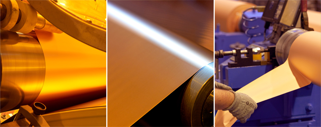
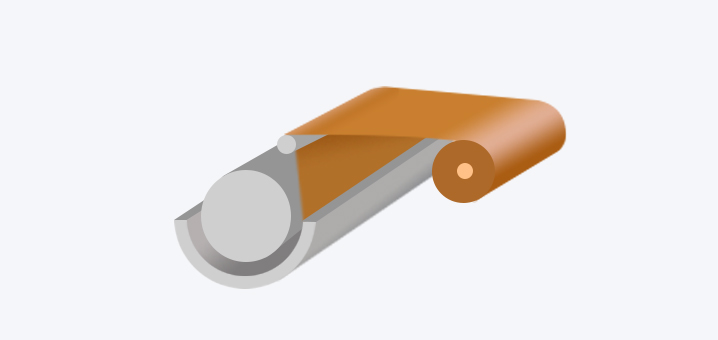
High-end copper foils created with the world's top technology
Copper foils are a key material for advanced industries, including artificial intelligence (AI) accelerators and radar for autonomous driving.
As the only copper foil manufacturer in Europe, Solus Advanced Materials continues to lead the global market, on the strength of our 65 years of manufacturing experience and expertise.
Business information
Shaping the AI era with high-end copper foils created by the world's best technology.
The key to making copper foil is to ensure that it has a uniform roughness while still providing good adhesion to the insulating film.
We have secured ultra-thin manufacturing technology down to 1.5 ㎛, contributing to advanced microcircuits, high integration, and multi-layering of PCB boards.
Recently, Solus Advanced Materials has been recognized by the large global tech companies for its copper foil products used in AI accelerators.
Strength
- HVLP Copper Foil
for AI Accelerators -
- We manufacture copper foil that minimizes signal loss by achieving a roughness of 0.4 μm (Rz JIS) with uniform surface treatment technology. This foil is applied to artificial intelligence (AI) accelerators and other applications.
- Holding the world’s leading thin foil manufacturing technology
-
- Manufacturing Ultra-thin products of 1-2㎛, having manufacturing methods suitable for making high-end PCB (Electronic circuit board) micro-circuit, highly sensitive and integrated, and multi-layered
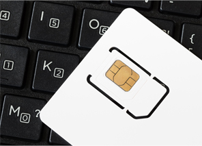
- Exclusive global supplier of copper foil for IC/USIM cards
-
- Our copper foil products are made with a manufacturing technology that ensures high strength and high elongation, and with a special surface treatment technology that prevents damage from external environments such as moisture, making them quite suitable for IC cards and USIM cards, and we are the exclusive supplier worldwide.
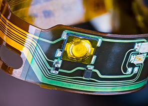
Product applications
- Multi Layer Board for AI Accelerator

- PKG Substrate for Semiconductor
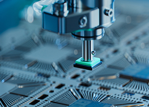
- Flexible PCB
- Aircraft

- satellite communication

- IC, USIM card
- Communication Base Station Radar
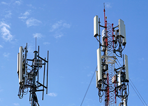
- Autonomous vehicle radar

Main Product
-
- Hyper Very Low Profile (HVLP) (BFL-NN-Z, BFL-NX-Y)
-
- Low surface roughness
- Has stable peel strength characteristics (over 0.5N/mm) with roughness of 0.4um or less (JIS standard)
- Used in AI semiconductors and network substrate materials for high-efficiency signal transmission
- Used in 5G communications equipment and Radars for autonomous electronics
- HVLP4 and HVLP5 development is complete
- Thickness : 9~35um
-
- Ultra-thin foil (DTH-N-TZA, DTH-ANP)
-
- The 1.5um~5um thin product can be used for IC Packaging and HDI application.
- Can be used for Modified Semi-Additive Process, applicable at Line Space of 30/30um and below.
- Dedicated facility for mass production in operation
- Thickness: 1.5~5um
-
- For Smart IC (LPT-TZA, LPT-NP)
-
- Copper foil for Smart IC
- High-strength, low-profile copper foil
- Optimized for reel-to-reel processes
- Excellent flatness characteristics for mounting high-performance IC chips
- Thickness: 18~70um
Manufacturing process
-
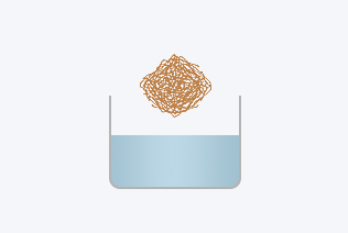
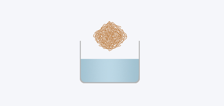
- 1. Dissolving
- Process of preparing electrolyte for plating
-
- 2. Plating
- Process of producing copper foil of uniform thickness by plating Cu ion on drums in electrolyte solution
-
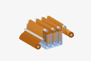
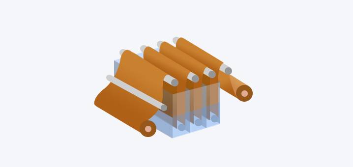
- 3. Treating
- Process of roughening the copper foil surface and enhancing performance through coating and other treatment
-


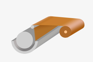
- 4. Slitting & Sheeting
- Slitting in the width direction of the copper foil according to customer demand size
-
- 5. Inspection & Shipping
- Process of packing and shipping after quality inspection
Product classification
| Product category | Subcategory | Product name | Application | Characteristics |
|---|---|---|---|---|
| HVLP (Hyper Very Low Profile) | HVLP5 | BFL-NF | Substrate materials for high-performance AI accelerators | Nodule-free technology. The best signal transfer characteristics available |
| HVLP4 | BFL-NX | Substrate materials for high-performance AI accelerators | Ultra-fine nodule treatment. Signal transfer improvement | |
| HVLP3 | BFL-NN | Substrate materials for high-performance AI accelerators | Ultra-low roughness (<0.6um) and excellent adhesion strength Suitable for high-performance AI accelerator boards with excellent signal transmission characteristics |
|
| HVLP2 | BF-ANP | Substrate materials for digital equipment for ultra-high speed transmission | Excellent adhesion at very low roughness of 1.0um or less | |
| HVLP | BF-TZA | Substrate materials for digital equipment for high speed transmission | Excellent adhesion to substrates with low loss characteristics and very low roughness | |
| BF-HFI-LP2 | Substrate materials for digital equipment for high speed transmission | Excellent adhesion to substrates with low loss characteristics and very low roughness | ||
| RTF (Reverse Treated Foil) | RTF3 | TZA-B3 | Substrate materials for digital equipment for high speed transmission (copper foil for reverse surface treatment) |
Product for reverse surface treatment Lower roughness than RTF2 products Best signal transmission characteristics among existing RTF products |
| RTF2 | TZA-B2 | Substrate materials for digital equipment for high speed transmission (copper foil for reverse surface treatment) |
Product for reverse surface treatment Enhanced signaling characteristics with lower roughness than default RTF products | |
| RTF | TZA-B | Substrate materials for digital equipment for high speed transmission (copper foil for reverse surface treatment) |
Reverse surface treatment on general foil to realize low roughness while securing price competitiveness | |
| PKG | - | DOUBLETHIN-CL | For IC boards and high-level multilayer integrated circuits | Ultra-thin foil for ultra-fine circuits specialized for ETS processes |
| DOUBLETHIN-NN | For IC boards and high-level multilayer integrated circuits | Ultra-thin foil for semiconductor substrates with next-generation microcircuit designs | ||
| DOUBLETHIN-ANP | For IC boards and high-level multilayer integrated circuits | Increased ability to realize microcircuits by reducing surface roughness (<0.9um). | ||
| DOUBLETHIN-N-TZA | For IC boards and high-level multilayer integrated circuits | Ultra-thin foil product with 1.5um/2um level, suitable for implementing microcircuits on semiconductor substrates | ||
| High Frequency | For fluoroplastics | BF-HFA | For Radar/LiDAR in base stations and electronic equipment | Achieves excellent adhesion to fluoroplastic substrates with low roughness |
| For specialty resins | TWLS | Radar for base station and electronic equipment; for special materials | High adhesion to resins with special systems such as hydrocarbon, PPE/PPO, etc. | |
| SMART-IC | - | LPT-NP | For materials for smart card / tape carriers | Excellent elastic modulus properties and high mechanical properties |
| LPT-TZA | For materials for smart card / tape carriers | Excellent elastic modulus properties and high mechanical properties | ||
| FLEXIBLE | - | BF-TZA-FX | For flexible substrate materials | High mechanical strength and high adhesion to polyimide films |
| AEROSPACE | - | TZA-TZA | For lightning protection on aircraft, wind turbines, etc. | Best adhesion strength with double-sided surface treatment |
| REGULAR MLB | - | TZA | For materials for general multilayer substrates | High elongation at high temperature and heat resistance |