Leading display revolution through technological innovation.

The Electronic Materials Business Unit researches, develops, and produces light-emitting and non-emitting materials used in organic light emitting diodes (OLED) displays.​

For over 15 years, Solus Advanced Materials has been developing its own OLED materials, functional new materials, and quantum dot materials through continuous research and development. Solus is now leading the global display materials market and continues to expand its business scope.​

Business information

Leading display revolution through technological innovation.

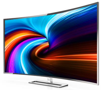
Organic Light Emitting Diode (OLED) is a display device consisting of organic emitting compounds.

Thin, light, flexible, and transparent display suitable for car display and AR/VR.

Used for illumination as well since it emits light similar to natural light.

Solus Advanced Materials has independently developed OLED materials, new functional materials, and QD materials through continuous R&D for over 10 years, leading the global display materials market. It also plans to expand its business lines steadily by developing products for materials for electronic devices related to the 4th-generation industries, including semiconductor chips and battery.

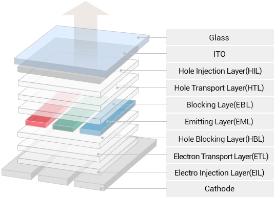
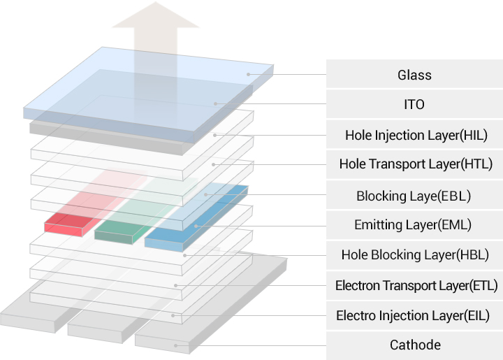
Structure of OLED

OLED (Organic Light Emitting Diodes)

The OLED display has the advantages of high luminance and efficiency as well as wide viewing angle that provides excellent color expression.

In addition, it has high operation speed and it can be driven at low voltage. A thin, multi-type display can be created as it emits light without the need for backlight.

Strength

Having core technology and patent for high efficiency/low voltage/long life
  • Holding numerous patents for organic materials with high efficiency/low voltage/long life, manufacturing and supplying massively (HBL, ETL)
  • Development of ET common layer material technology for small and medium-sized devices and next-generation tandems​
  • Long-life materials achieved through deuterium technology​
  • Synthesis development using AI simulation, securing 200 material pools
Supplying customized products
  • Developing/Supplying customer-specific materials through joint development/collaboration and correlation
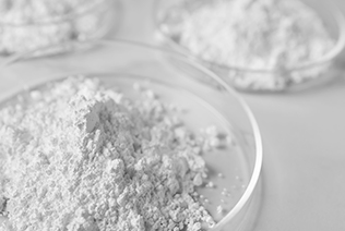
  • Supplying after molding by type required by the customer (Powder/Granule/Stick/Coin type)
Securing optimal manufacturing/quality control processes
  • Securing high-purity quality and optimized operation of the mass production process
  • Securing uniform product quality by operating advanced quality control system for each process
  • Aligning the quality standard with customers
Future technology development and investment
  • Investing in and developing future display technology
  • Holding a number of future technology patents such as functional polymer/QD

* QD: Quantum Dot

Product applications

  • Light-emitting materials for smartphone OLEDs​
  • Light-emitting/non-emitting materials for OLED TVs​
  • OLED materials for vehicles​
  • OLED materials for IT such as tablets/PCs​

Main Product

  • HBL (Hole Blocking Layer)
    • Has been supplying to major customers at home and abroad since 2015
    • When our HBL is used,
      driving voltage -0.54V, efficiency +45%
  • ETL (Electron Transporting Layer)
    • When our ETL is used
      efficiency 130%, lifespan 105%,
      driving voltage -0.45V
  • EML (Green Host)
    • Mass production testing at customer sites during 2022-2024​
    • Mass production and promotion of high-performance entry-level materials in progress
  • Filler
    • Our fillers have been supplied to major Korean customers since 2020​
    • Our fillers are:​
      Highly refractive (RI ≥1.60) materials to increase light extraction efficiency​
      Characterized by high reliability and high adhesion, securing the reliability of the panels​

Manufacturing process

  1. 1. Synthesis
    High-purity products are manufactured by an exclusive facility for each product.
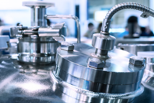
    • Synthesis: Manufacturing products using reactants and catalysts, etc.​
    • Wet purification: Producing high-purity products through column chromatography, recrystallization, etc.​
  2. 2. Sublimation/Refining
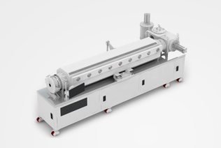
    High purity and yield are secured by the patented facilities of the company.
    • It is possible to eliminate impurities to the maximum by adjusting the temperature in each internal section.
    • It is possible to minimize temperature damage to the product by refining it in high-vacuum.
  3. 3. Forming/Packing/Shipping
    Products are shipped after forming them in the shape desired by the customer, such as the Stick or Coin type, using a powder molding machine.

Product classification

Product classification & features
Product name Characteristics
HBL(Hole Blocking Layer)
  • Mass-producing and supplying to major customers
  • Secured high performance light extraction efficiency performance
  • Holding outgas-free production technology
ETL(Electron Transporting Layer)
HTL(Hole Transport Layer)
CPL(Capping Layer)
EIL(Electron Injection Layer)
Inorganic materials
Blue/Green
  • Development based on the premix prediction system
  • Secured the technology of optimizing host-dopant combination performance
  • Holding technology for low voltage driving NGCL materials
Functional polymer materials
  • Integrating functional monomer design and synthesis development
  • Optimal mixing and composition technology for each curing method
QD(Quantum Dot)
  • High-efficiency, high-purity QD and ink composition technology
  • Integrating QD-EL element technology combined with OLED material technology

R&D

Solus Advanced Materials is developing materials based on data accumulated for many years.
Solus Advanced Materials is continually communicating with customers to develop materials suitable for the performance desired by the customer and conducting efficient and effective R & D activities using simulation equipment.
Solus Advanced Materials is also conducting research on future technologies that will lead the display market in the future, and it holds numerous related patents.

R&D

Products
Development
  • Derivation of new structure through IP analysis
  • Customized development through joint development with customers
  • Utilize AI-based simulation system
Process
Engineering
  • Development of optimized synthetic purification process
  • Scale up process development before mass production
Future
Technology
  • Development of post OLED materials (QD, perovskite)
  • Development of Inkjet Printing polymer materials
  • Joint research on future technologies with customers
Device
Development
  • Device Evaluation and Material Combination
  • Matching element structure with customers

Contact information

Battery copper foil

Domestic/Overseas sales
Inquiry

Copper foil

Domestic sales
Inquiry
Overseas sales
Inquiry

Electro Materials

Domestic sales
Inquiry
Overseas sales
Inquiry

BIO

Cosmeceutical Ingredient
Inquiry
Pharmaceutical Ingredient
Inquiry
Nutraceutical Ingredient
Inquiry
CDM business
Inquiry
페이지 상단 이동